The designers, engineers, and builders of today’s megafabs are turning to augmented reality and shared data hubs to ramp smarter facilities with record-breaking speed.
2024.10.11
AI and robotics are taking on bigger, more complex, and increasingly autonomous tasks, but integration with existing equipment and processes remains a formidable challenge.
Pros and cons of a middle-ground chiplet assembly that combines 2.5D and 3D-IC.
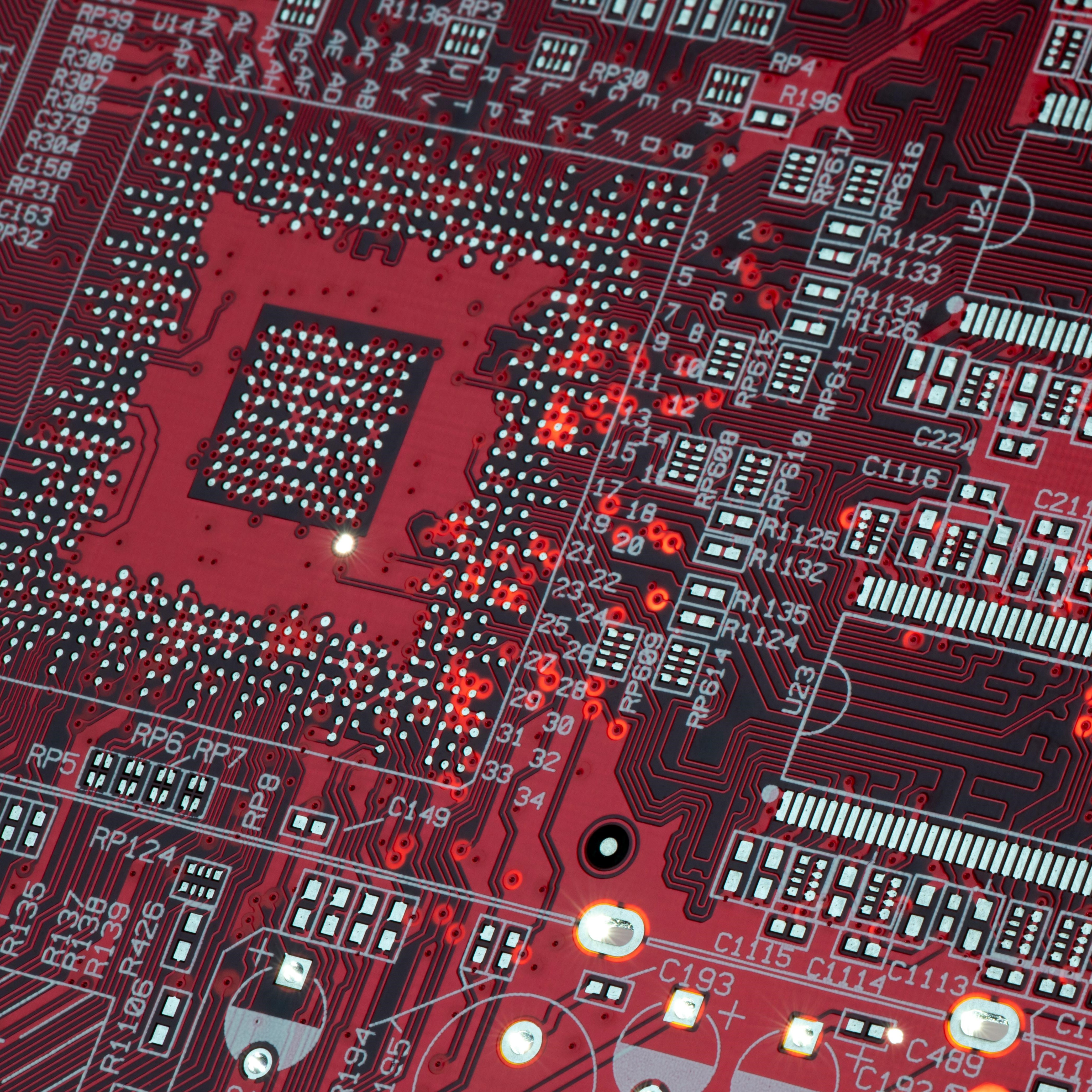
Controlling interference in today’s SoCs and advanced packaging requires a combination of innovative techniques, but new challenges emerge.
Development methodologies combine old and new techniques, but getting any new material into high-volume manufacturing is a complex process.
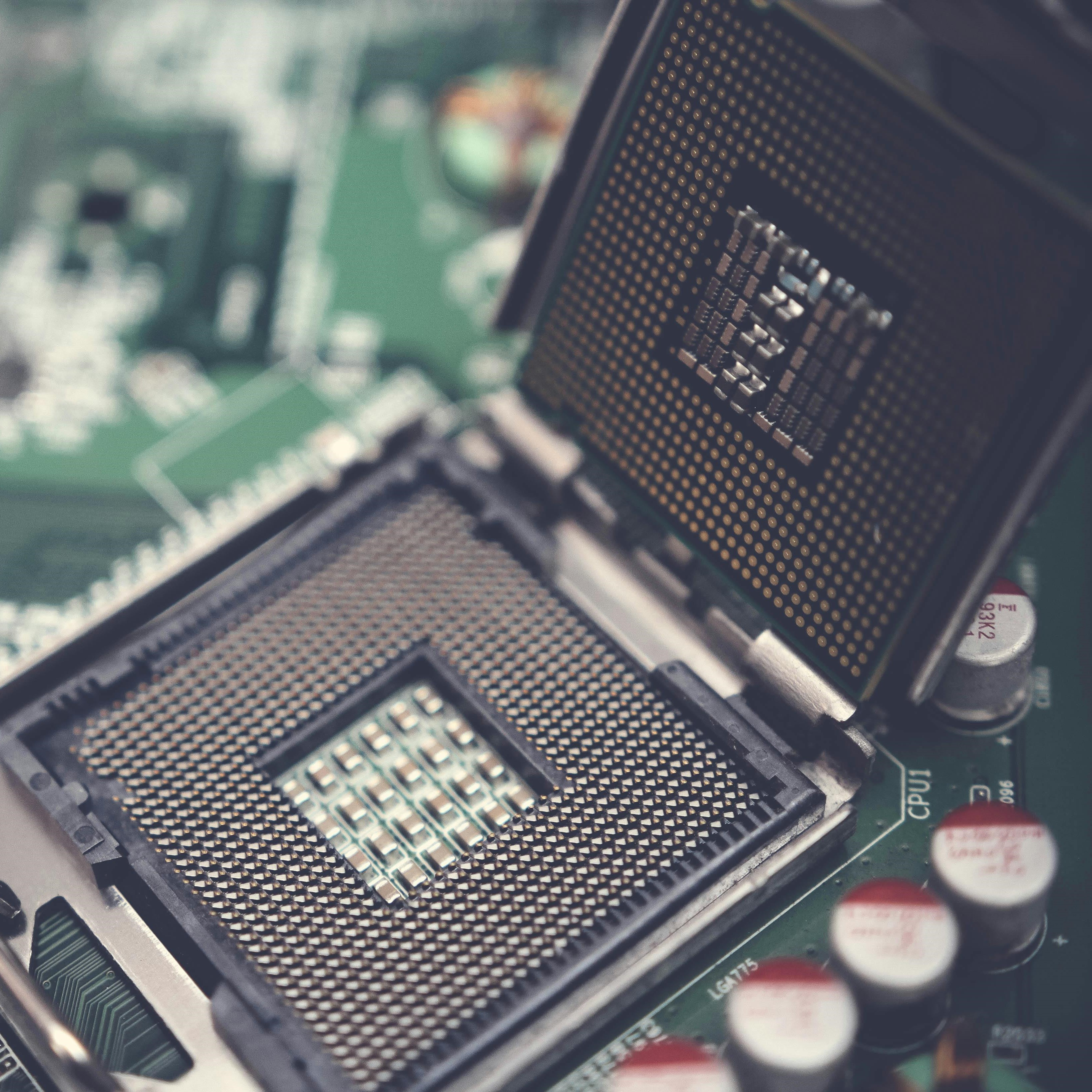
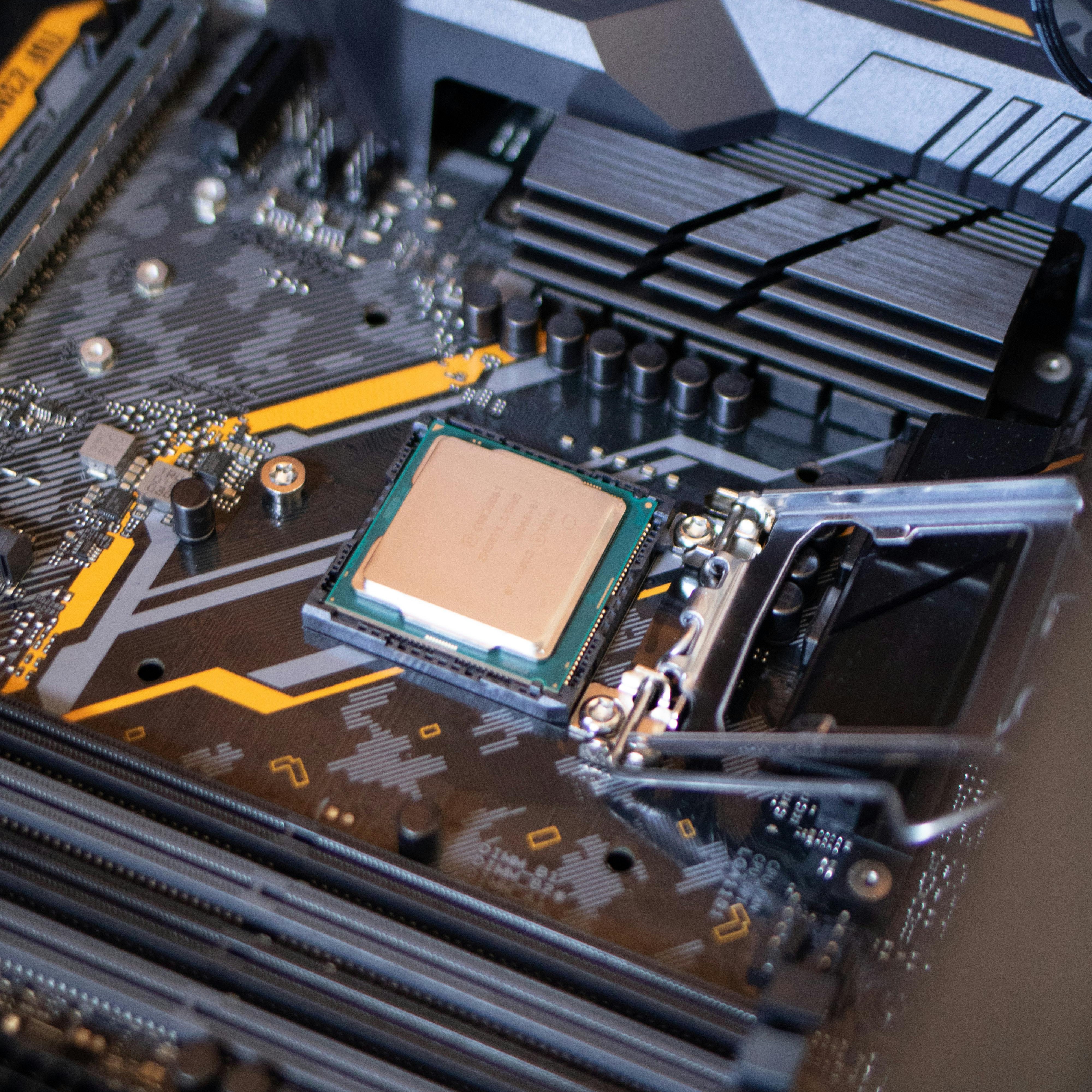
Chiplet-based products must accommodate small differences in die size and bump pitch, placing new demands on manufacturing tools.
Several critical processes address wafer flatness, wafer edge defects and what’s needed to enable bonded wafer stacks.
How chiplets and advanced packaging will affect power efficiency, and where design teams can have the biggest impact on energy consumption.
2024.09.22
It’s been decades since there was a disruption within EDA, but AI could change the semiconductor development flow and force changes in chip design.
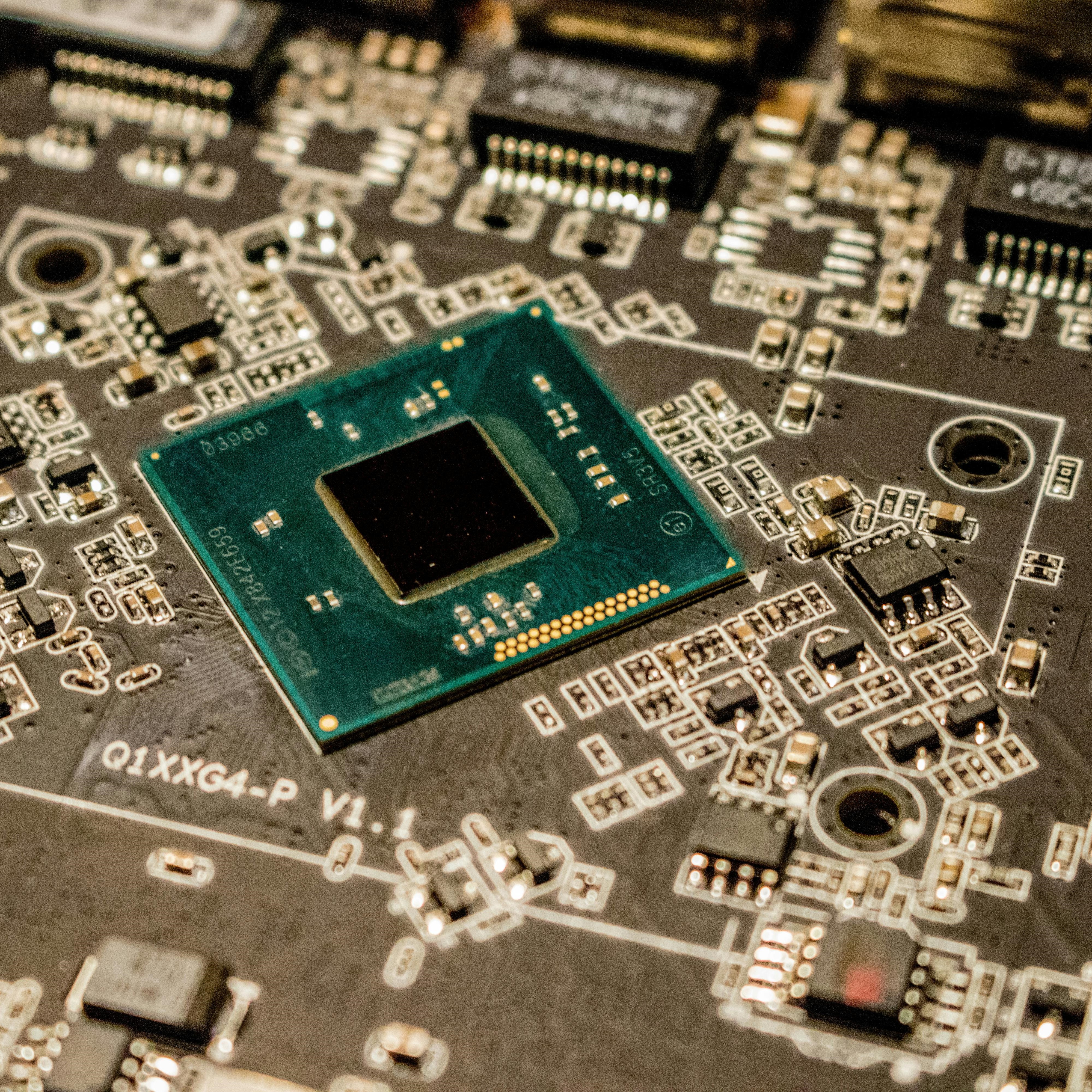
Megafabs churning out the most advanced processors are not the only game in town.
As vulnerabilities become more widespread and better known, industry standards will have to keep up.
Researchers and engineers are working on increasingly secure processes in the EDA workflow, but they add to the cost.